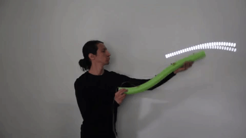
The IMU Noodle
IMU Noodle–what’s that? Just a testament to a world that’s filled with a rich ecosystem of MEMs sensors to play with!
The BNO055 is one of these sensors. Not only does it contain an 3-axis accelerometer, gyroscope, and magnetometer, it also contains an onboard microcontroller that processes this data to estimate orientation. With a little extra bandwidth after-hours and a few custom PCBAs, I whipped together a project that’s been calling my name for years.
With a handful of these MEMs sensors and a little quaternion math, I present: the IMU Noodle, a motion capture device designed for following the contours of flexible 3D objects.
The Why
In the 6 or so months before this project, I churned out half a dozen PCBA designs for work. I figured, with all that practice, why not put my newfangled skills to good use and spin a few PCBAs for fun? The IMU Noodle Node is the first board in this installement, and I hope to churn out a few more in the coming months.
Core Design Concept
The IMU Noodle is a cluster of imus strapped onto a flexible object to estimate its 3D curvature. Each IMU spits out its orientation encoded as a quaternion with an update rate of 100Hz. With a little math in software, I’m assuming a fixed length between nodes, interpolating the node-to-node curvature, and finally plotting it at a crisp 60Hz.
I tried very hard to be patient with this project’s hardware. I figured: if I do it right, I can re-use some of the core ideas for future node-based projects. Here’s the breakdown.
Adding I2C Addresses
Problem: the BNO055 has only two, fixed options for I2C addresses. Contraint: I need to keep the number of wires running out to these nodes down to a minimum; in fact, a shared bus would be ideal. The Solution? Behold, the LTC4316 “I2C Babelfish.” This little nugget of joy takes three (or four) configuration resistors as input and re-encodes a device’s I2C address on-the-fly. It does this by isolating a run of the I2C’s signal wires and re-translating all addresses downstream. In my case, I’ll devote one of these chips per PCBA such that I can re-encode the I2C address to a different value of my choice, dictated by the values of three resistors.
For the curious, I have much love for this chip, so I wrote up a few more details elsewhere.
One Shared I2C Bus
To communicate from board to board, I wanted a single I2C bus. In principle, this means I can share the same wires across all nodes. In practice, the electrical specs of I2C just don’t support being run over long wires. I2C is intended to stay locally onboard a single PCB since the signal wires are “open-drain,” making them too weak for long cable runs, and I need these nodes to run out to a meter or two. The solution was differential (D)I2C. Here, the protocol to communicate with each node follows the conventional master-slave interface of I2c, but the signal runs over two differential pairs. The benefit of this differential encoding is that it’s far more noise-immune to EMI, letting me pass this signal over about 3 meters of cable without needing to worry about noise that could otherwise flip bits or lock up the bus.
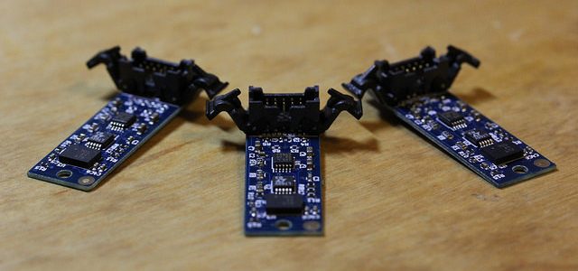
One Configurable PCBA
I knew I wouldn’t be patient enough to solder 10 of these by hand, and I knew that no professional assembly house would be willing to make 10 unique boards on-the-cheap. The solution? I needed to design one PCBA such that, with minimal tweaking, I could configure it with a unique I2C address from the batch of 10. Overall, I’m trying to save myself from all those chances where my finicky fingers could make a costly mistake–not to mention sneezing away countless SMD parts in the process. This PCBA has 3 resistors that I left out of the Assembly BOM so that the assembly house doesn’t populate them. With these 3 resistors, and a handy-dandy resistor booklet from 10K to 97K, I can selectively hand-solder them to create a voltage divider that dictates the device’s I2C address.
Firmware and Software
As far as software goes, I’m using a Teensy to poll each IMU at 120 Hz and then stream all that data into the computer through a USB HID interface. Data enters the PC in two packets at about 60Hz–perfect for visualizing on a normal display monitor! To visualize the data, I wrote up a snippet of interpolation code and plotted it in real time using OpenFrameworks. By far, my favorite part about choosing OpenFrameworks for the visualization is that it compiles on some smaller single-board computer platforms out there, like the Raspberry Pi, which means I could someday deploy a dedicated Pi to a TV set as an art installation!
Quaternion Math
At some point, I realized: wow, I could write an entire post on just how wonderful quaternions are for the math behind this project–so I did just that in my Motion Capture of All-Things Bendy post.
Scaling Down
Getting these BNO055 chips on a breakout board wasn’t too tricky since Bosch kindly provides a suggested application schematic.
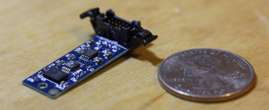
As for what’s on the board, there are 4 main features. First off, the PCA9615 does the heavy-lifting of translating the differential signals back into an open drain configuration. FIX THIS SENTENCE. Next, the LTC4316 dynamically re-encodes the I2C address to a different one in the available address space. That address is actually set by the raw voltage values sensed across a resistor ladder that I solder up by hand after the boards come back from the assembly house. Finally, the BNO055 does all that nice sensing and filtering that would’ve otherwise been another month or effort.
With 3 ASICs, the board is a bit crammed, but there’s still room for a bit more size optimization.
A Mini Production Run
On the assembly side, this is the first time I have a professional assembler populate a set of PCBAs for a not-work side-project. (Now, before you penny-pinching hackers shake your fists at me, hold up: I can reflow TSSOP packages with a hot plate and a stencil like nobody’s business. I just didn’t want to deal with the headache of diagnosing 10 almost-working boards.) I’ve failed one-too-many times with other mini QFN-size packages that I figured, with my time cut short from work and rock climbing, I ought to enlist some help to do a quick run of 10 of these PCBAs. (I ordered extra boards and a stencil for practice later.)
After getting some recommendations, I picked PCBWay for this assembly adventure. For a run of 10, these boards were $61.50 a pop. That might not seem cheap, but the actual component cost is about $20. For such a tiny volume of 10 boards, $40 per board for assembly services is not bad. (Darn–looks like that new Nintendo Console I’ve been swooning over is going to need to wait a few months.)
For most other side projects with just a single PCBA, professional assembly isn’t really an option. With all the hassle of finding a vendor that will (1) keep the up-front cost down and (2) even agreee to assemble a single board in the first place, we after-hours engineers are usually better off assembling it ourselves. Fortunately, with this project, I actually did need multiple PCBAs, all of which were mostly identical! Now that sounds like a pretty good option for outsourcing the assembly.
Ruling out Uncertainty
At some point, the price for mistakes in hardware is real money (and, of course, added time, extra head-scratching, and more confusion). These days, I’ve been humbled by enough wrong assumptions to test as many independent subsystems in isolation as possible. For this round, my biggest unknown was finding a bulletproof way to run the I2C protocol over a long cable.
After a bit of research, behold: the PCA9615, a differential transceiver specifically intended for doing just that! This golden nugget re-encodes the I2C bus onto two differential pairs. Between two of these PCA9615s, we can run a long cable in a way that’s protocol transparent, which means my IMU nodes literally have no idea that their bits are getting encoded to a different electrical spec and then de-coded back again before being read. What’s more, this chip supports a “multi-drop” feature, meaning that any number of PCA9615s may be dropped along the length of the differential cable to connect onto the same bus. The PCA9615 takes the principles of I2C (unique slave addresses, a shared bus), and pushes the analogy forward from inter-chip communication to inter-board commmunication over a shared bus.
Now, this all sounds too-good-to-be-true, so I just had to test it. I spun a few cheap soldermask-free boards to break out these chips and get comfortable using them to make my I2C bus longer.
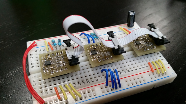
Ta-daa–it works! Now I can commit to popping them onto my BNO055 breakouts.
Aside: The Engineering Vacuum
It’s easy to forget just how many other engineers have probably had this exact problem: extending the I2C bus over loong wires. Usually, finding an all-in-one solution in the form of an ASIC tells me that I haven’t strayed too far off the deep end of the design space. In contrast, when my needs get so niche that my searches can’t find any leads, that’s a good sign that I’m not tackling the problem from the right angle.
Here lies the “trade-secret engineering conundrum”: so many engineers keep their designs closed from the rest of the world, wrapped under an NDA; wouldn’t it be exciting to see just how much farther we could push the field if we shared our designs, rather than keeping them to ourselves? As far as learning goes, this style of engineering seems to be at odds agains the noob engineer. Without a senior engineer to slap the back of our hands and say “don’t design it that way; do it this way,” we’re left to fend for ourselves to try to converge on the same solution as another engineer who’s already solved this exact problem at another company. Nevertheless–we engineers are problem solvers. Odds are good that we’ll still stamp out a final product that works at the end of the day.
What’s frustrating about this scenario is the attitude that it tends to introduce into the community. When two engineers gather after hours to discuss their work, we high-five each other for independently converging on the same solution, as if we now both silently approve of each other’s “smartness” for building the same widget that gets us through the same trial by fire.
I do bemoan the secret independent “re-invention of the wheel” at various companies when we could be rolling out on something much more interesting, but I’m not yet sure how to address this issue.
As far as solving this particular problem goes, I’ve written down my research efforts here to spare you a few extra hours. May they serve you well.
Wiring it Up
A shared I2C bus means I don’t need to run a pair of wires for every single node. To make that happen, I picked a teeny ribbon cable variant so that I could clip in connectors anywhere along the cable.
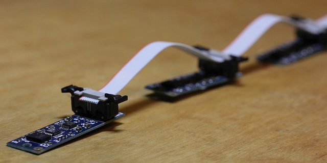
These connectors are about the cutest hardware component I’ve seen this year–the pics just don’t do it justice! For the curious, the part numbers are as follows:
- Connector: 45110-010030
- Socket: 45210-620230
- Cable: 517-3754/10
Into The Wild World
These days, my best way of testing the ruggedness of my side projects is to put them into the hands of other folks to try for themselves. I’m thrilled that the IMU Noodle has survived its first after-hours excursion down at the Post-Maker Faire Bring-a-Hack Dinner brought to us by OSH Park.
See you at the next Maker Faire!
Finally, yes, if you’re thinking: tentacle, then stay tuned.
PCBA Files and More
- PCBA Files and Source Code
- The Flickr Build Log
- Previously on Hackaday: Taking the Leap Offboard: an Introduction to I2C over Long Wires
- Previously on Hackaday: An Introduction to Differential I2C
- Previously on Hackaday IMU Noodle Nodes to Motion Capture All-Things Bendy