PCB Etching
The Toner Transfer Method for single and double-sided PCBs
Introduction
When I began the leap into digital electronics, I believed that the only limit to what I could design and build would be my imagination. I quickly learned,though, that it was actually the breadboard. I longed to spin my own boards for permanent projects, but I wasn’t yet confident enough to take a breadboarded project, design a printed circuit board implementation, and send it out to be fabricated on a whim.
To gain some confidence, I began etching boards to bring a project from start to finish. While sending out the board is the real finishing point to a project, I’ve found that etching still has a place as a method of fast prototyping.</p>
To the hobbyists, pcb etching enables us to communicate with a number of additional chips only available in surface-mount packages. It also enables fabrication of breakout boards for these surface-mount components for testing on a breadboard.
Actually realizing this dream of etching DIY boards took two years to finally nail. While a number of other electronics gurus make the process seem straightforward, there are a number of undisclosed pitfalls that I learned the hard way. As a result, I’ve done my best to outline my own workflow for etching boards. I hope these notes serve future digital designers.
Etching boards is still an ongoing learning process for me. As I learn more, I’ll continue to keep this page up-to-date.
Materials
Cupric Chloride: How not to annihilate the environment with every board
A number of hobbyists etch circuit boards with ferric chloride, a classic and very effective etchant. Unfortunately, the waste product of each board is toxic and unusable. This waste etchant must be disposed through proper hazardous waste management, a process that often involves a charge.
An alternative to ferric chloride is cupric chloride. Cupric chloride, aka copper(II) chloride, is formed by reacting hydrochloric acid with oxygen and Copper. This process must be performed in a well-ventilated area (ideally: a fume hood) as the reaction can give off chlorine gas as well. The product: a solution of cupric cholride, can be used as an etchant.
Cupric chloride has a strong advantage over ferric chloride for it’s renewability. Post-etching, the cupric chloride solution can be aerated to be renewed and used for etching boards repeatedly. The reaction with copper actually produces more etchant, effectively concentrating the previous solution and resulting in faster etchings with the same solution. Yes, over time, copper(II) chloride dihydrate may precipitate when the solution becomes saturated. At this point, some of the solution can be disposed of through hazardous waste management, and the rest can be diluted to continue etching more boards.
Toner-Transfer Material: Vinyl
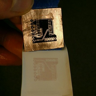
The process of the toner-transfer method is, quite literally, to take the toner (dusty ink) from a laser printer and transfer it onto a copper-clad board. From that point, the copper beneath the surface of the toner will resist being etched (removed) by the etchant when the board is bathed in the etchant. All exposed copper will be etched away. Following the etchant bath, the toner can be wiped clean, exposing the untouched copper beneath.
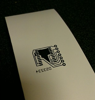
Since it’s not feasible to print the resist pattern directly onto a pcb, a decal of sorts (a transfer material) must be used as an intermediate step. The process is as follows:
- Print pattern out of toner onto transfer material.
- Transfer the toner off of the transfer material and onto the copper-clad board using heat.
- remove transfer material without leaving any of the toner on the transfer material.
The process seems straightforward, but many transfer materials often perform and imperfect transfer onto the copper-clad board, leaving small ripped pieces of the pattern behind. A number of people have tried printing onto different materials giving different levels of satisfaction. Originally, magazine paper was the manner by which this process was done, since the toner would not adhere to the glossy surface of the magazine pages. However, very steady hands are needed to not smear the pattern as it is placed onto the copper-clad board. Since slipping and smearing the pattern can become frustrating, other transfer materials have been investigated. </p>
In my opinion, by far, vinyl (as in vinyl used by vinyl-cutters for sign-making), is undoubtedly the most reliable transfer material. Since the pattern actually weakly sticks to the vinyl, steady hands aren’t needed to prepare the pattern to be transferred onto the copper-clad board. Furthermore, when heat is applied to the vinyl, it becomes soft, readily permitting the toner to leave the vinyl and adhere to the copper-clad board instead. The folks over at electroni-city.com have made this discovery, and they definitely deserve recognition for this find.
Uber-Tiny Drill bits
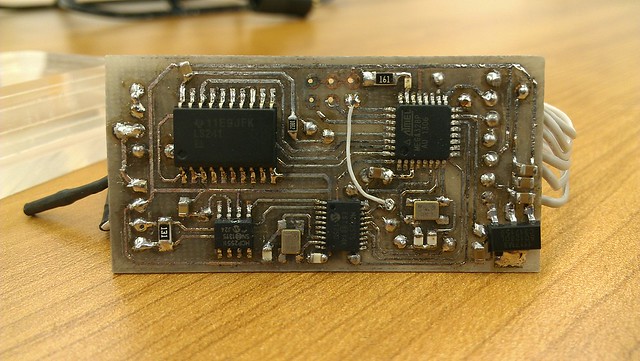
To drill out the via and through-hole component holes, a set of tiny drill bits will do the trick. Sizes 68 through 78 should work for most boards, though I typically only use three from the set: #68 and #70 for through-hole components and #72 for vias. If inserting a tiny drill bit into a drill press or dremel chuck is a problem because of their width, these drill bits can also be purchased with an 1/8th-inch shank from McMaster-Carr.com, making them easier to clamp. Since drilling these holes takes some decent hand-eye coordination that I don’t always have, I tend to try to stick to strictly surface-mount components and minimize the number of vias to overall minimize the holes that I’m drilling. (Believe it or not, when armed with tweezers, surface-mount soldering is actually easier than it looks, plus your boards look way more professional and have a thinner profile from mostly flat components.)
Painter’s Tape
Under high heat, other tapes tend to melt. Painter’s tape, however, survives the pattern transfer heating process without any problems. It also does the trick of sticking just securely enough to hold the pattern while also being weak enough to remove by hand. Finally, it softens under water, allowing it to be more easily removed.
Design Guidelines
Routing Angles
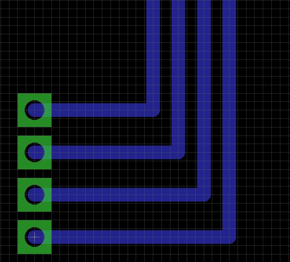
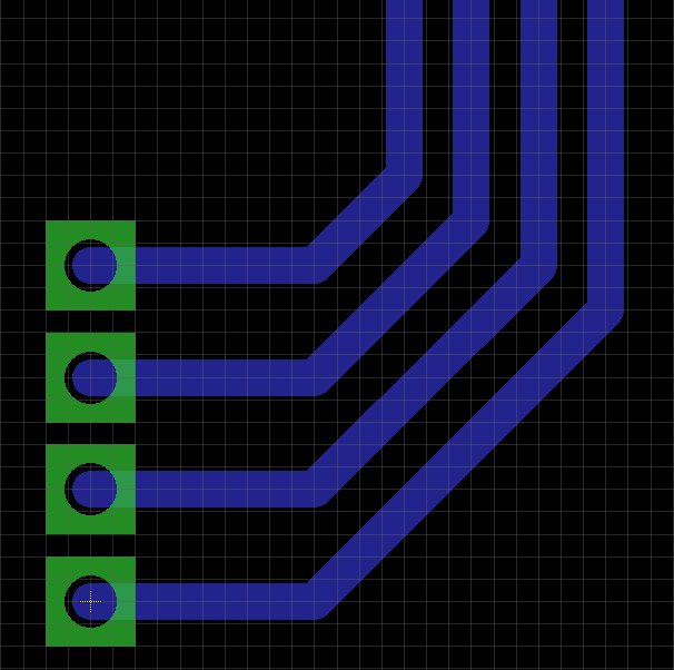
In developing a DIY board, it’s best to avoid 90-degree angles. According to forums and a few others far more skilled that I, etchant tends to remain in the corners, which corrodes the corners more noticeably than angles that do not have the 90-degree feature. In the images below, I tend to route traces with 45-degree bend such as those on the right-hand side.
Filling The Remaining Plane
With the Polygon tool in Eagle, I’ll add a plane that is electrically connected to ground. This reduces etching time, since less copper is exposed to be removed from the board. For a double-sided board, dedicating the bottom plane to ground may reduce electromagnetic interference (EMI); however, that plane cannot have any “moats” or other isolated sections to actually be beneficial.
Effectively reducing EMI involves far more complicated rules to abide by for board layouts, but this document gives an overview about some aspects to consider.
Pattern Transfer
For a double-sided board, aligning the board can be one of the trickiest steps. Once done correctly, the results are quite stunning. To perform the alignment, I use vias as alignment holes, which tends to work pretty well. (Hopefully, if I’m doing a double-sided board, there are bound to be vias, otherwise having a double-sided board starts to make a little less sense. In that sense, there should always be vias to a double-sided board to use this same trick.)
Printing the Pattern
Remember that the design software board layout generally provides an “x-ray” view of the board looking at it from the top through to the bottom. What this means for printing is that the decals should be printed as follows:
- The top layer is mirrored
- The bottom layer is unmirrored
Before printing, hide all layers except:
- top (repeat for the bottom, hiding top)
- vias
- holes
- board outline (optional)
Alignment
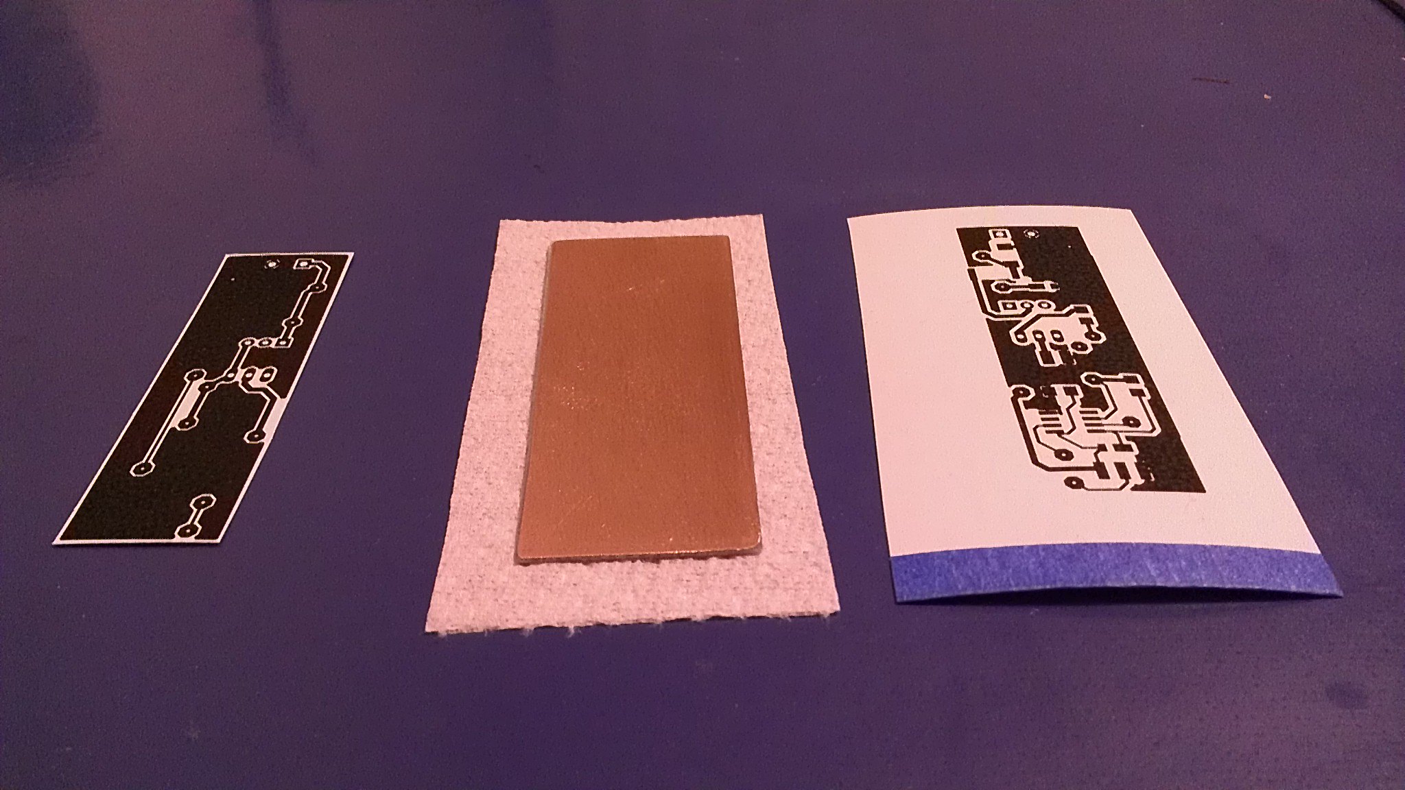
- Sizing is the first important issue here. To make the pattern easy to secure before entering the laminator, I will cut out the following sizes:
- One pattern layer is just the right size to hold the entire pattern.
- The copper-clad board is slightly oversize with a border of about 0.05” to 0.1”.
- The other pattern layer is way oversize to hold everything together.
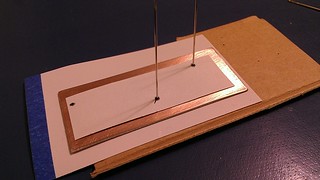
- Once the patterns and copper-clad board have been cut down to size, alignment holes must be made in each piece. I’ll first choose (at least) two vias. With a few sewing needles, I’ll prick a hole into the pattern using cardboard as a base to hold the pattern as subsequent holes are made.
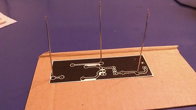
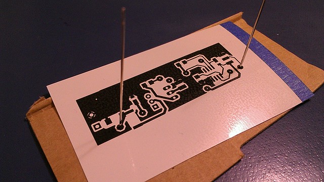
(Don’t forget that both patterns must be pricked with consistent holes.)
- Next, the same holes must be then drilled through the copper-clad board.
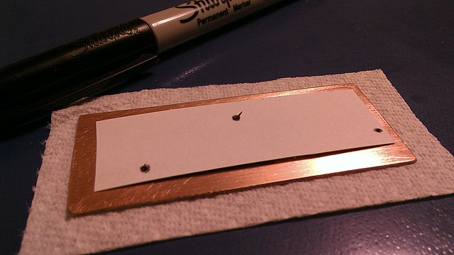
To do so, I’ll color the copper with a sharpie by using one of the patterns as
a reference. By holding the pattern flat against the board, a thin sharpie will
bleed through the hole to the copper, marking the spot to be drilled.
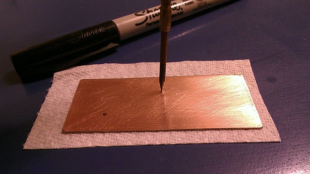
 Prior to drilling, I’ll first make a small indent using a metal poking tool
and a hammer. When drilling out the holes, the indent helps guide the drill bit
such that it begins drilling in the right location.
Prior to drilling, I’ll first make a small indent using a metal poking tool
and a hammer. When drilling out the holes, the indent helps guide the drill bit
such that it begins drilling in the right location.
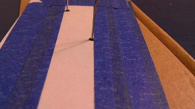
Securing the Pattern
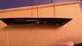
Once the holes have been drilled, the three layers can be aligned and secured
with blue tape. I slide the needles through one layer just far enough to hold
the other two layers, and then slip the other two layers in through the holes.
I’ll then push the ends of the exposed tips into cardboard to hold the pattern
as I secure it with tape.
When applying tape only apply it to three sides of the pattern, leaving one side exposed to remain as a starting point for removal. I also recommend creasing the tape down onto the pattern to ensure that it doesn’t slip as the three layers pass through the laminator for transfer.
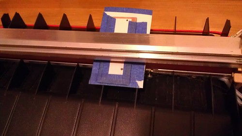
Transferring the Pattern
I pass the pattern through a laminator about 4 to 5 times. Following this procedure, I’ll immediately submerge the entire piece in cold water to “flash-cool” the piece. This rapid cooling process helps transfer the pattern off of the vinyl as the vinyl contracts slightly in response to the temperature change.
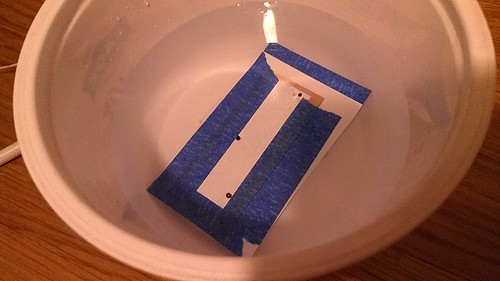
The painter’s tape can be sliced at the crease with an exacto knife. After the piece has cooled, I’ll gently peel away the pattern under cold running water.
Sealing the Pattern
The board, in its current state, can be etched, and will likely yield a
working circuit (er, provided that the design is sound). However, etching a
board in this state generally results in poor surface finish, as the etchant
tends to leak through the toner. The solution? Seal this layer of toner with
laser foil. I first saw this trick performed by
Paul Wanaker
Laser foil isn’t the only option here though.
pcbfx.com
sells toner reactive foils that do the exact same thing. While this isn’t an
advetisement for their product, this Green TRF foil appears to perform the
exact same task of sealing a board prior to etching.
Laser foil fulfills the task of sealing the board from the etchant far better than simply the toner alone. The foil sticks exclusively to toner from laser printers, making it ideal for use in pcb etching via the toner-transfer method. (The original use of laser foil is for awesome craft-making like homemade shiny cards.) The image below shows two boards: one etched with toner alone, and one board etched with both toner and laser foil as a sealant. The results not only make the laser-foil-sealed board more picture-worthy, they also preserve fine traces.
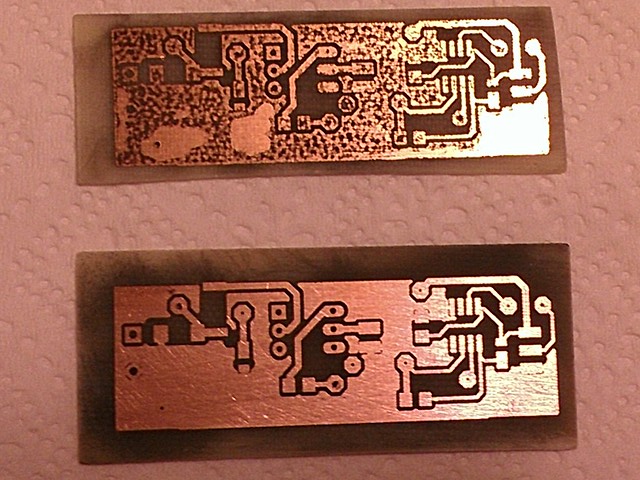
Notice that the upper board also has three splotches of fairly smooth copper where the pattern appeared to be well-sealed. As a test, I covered those areas with permanent marker prior to etching. Otherwise, they would’ve emerged pitted like the rest of the board.
The Etching Process
Etching can be made faster under warm conditions (slightly above 30 degree C). As The Real Elliot and Adam Seychell explain thoroughly, the etching reaction occurs on the surface of the board forming cuprous chloride. Consequently, agitating the board causes this thin layer of cuprous chloride to disappate off of the board surface and expose more copper to the etchant.
Questions or Comments? Feel free to send me an email.

This work is licensed under a Creative Commons Attribution 4.0 International License.